May 17, 2018 at 02:13PM
via IEEE Spectrum Recent Content
In the sci-fi addled popular imagination, the term “nanotechnology” conjures an image of nanobots assembling macroscale objects atom-by-atom. Whether these nanobots end up being the soft, biological variety or the hard, diamondoid version, the prevailing wisdom remains that it’s all still pretty far off.
Last month in the journal Nature Communications, we got a real-world glimpse into what nanoscale robotic assembly might look like—and it’s pretty close to being commercially available.
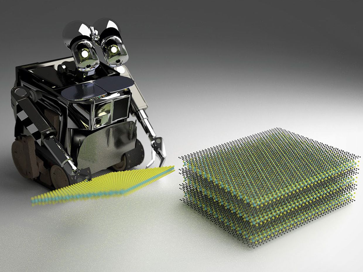
Japanese researchers have fabricated a system consisting of an automated optical microscope, a chip transfer robotic arm and a stamping apparatus that is capable of stacking two-dimensional (2D) materials known as van der Waal (vdW) heterostructures much more rapidly than humans can. These vdW heterostructures get their name because van der Waal forces hold the layers together. The unique property of these nanostructures is that by alternating the layers between conductors (like graphene) and insulators (like hexagonal boron nitride) it’s possible to give them tailored electronic properties, like specific band gaps were no electron states can exist.
This week in the journal Nature Nanotechnology, Riccardo Frisenda, a researcher at the Madrid Institute for Advanced Studies (IMDEA) and Andres Castellanos-Gomez, also a researcher at IMDEA, penned an analysis piece about this research that indicates this robotic system could not only be a game changer for nanotechnology research but also improve the prospects of large-scale nanotechnology manufacturing.
In their article, Frisenda and Castellanos-Gomez illustrate the potential of this system by using the example that it takes researchers days to assemble 13 layers of a vdW heterostructure while the system developed by the Japanese researchers can assemble 29 layers within 32 hours. Castellanos-Gomez told me that he believes this is just a starting point.
“The time it takes for the robotic assembly to work can be further improved by a lot,” said Castellanos-Gomez. “Right now one of the main limits for the speed is that at each transfer step the process is interrupted to ask for the OK of a human supervisor. The main reason for this human supervised step is that the alignment process has an uncertainty of 10 microns. By using motorized stages with better encoders (that technology is readily available) this human supervisor could be eliminated. I am pretty sure that that would speed up the process by a lot.”

Castellanos-Gomez sees this system as a kind of precursor to molecular mechanosynthesis, or at least in line with that proposed technology’s general aim.
“Instead of using the commonly used 'top-down' approach to fabricate small devices by sculpting a bulk material (e.g. in silicon industry the starting point is a macroscopic silicon wafer that is lithographed and etched to define very small transistors), in this work they use the 'bottom up' approach where a nanodevice is fabricated by piling up atomically thin layers,” said Castellanos-Gomez.
Of course, there are self-assembly methods for layering vdW heterostructures that do not involve researchers manually piling on the layers. However, these self-assembly methods are only capable of creating simple heterostructures (with alternating layers A-B-A-B-A-B), according to Castellanos-Gomez. In contrast, this new robotic technique can be easily used to produce heterostructures as complex as the user wants them.
If this robotic system is to move beyond merely making life easier for lab researchers and get into large-scale manufacturing, it will have to demonstrate its compatibility with large-area synthetic 2D materials grown by chemical vapor deposition (CVD) in order to make that jump.
“So far, the technique has been demonstrated to work excellently with exfoliated flakes of 2D materials,” said Castellanos-Gomez. “While this makes it limited to the lab use right now, I don't foresee any big technical challenge for its adaptation to be used with CVD materials in the near future.”
Whether it can make that leap to large-scale production will not necessarily hinder the system from becoming a commercially available. “The system right now looks pretty close to a commercial system,” said Castellanos-Gomez.
Castellanos-Gomez added that the system would benefit from electronic and mechanical engineering work in order to improve the reproducibility of the motorized stages used for the automatic alignment.
The Semiconductors Newsletter
Monthly newsletter about how new materials, designs, and processes drive the chip industry.
About the Nanoclast blog
IEEE Spectrum’s nanotechnology blog, featuring news and analysis about the development, applications, and future of science and technology at the nanoscale.